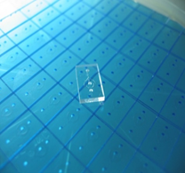
Foundry Service
Total One Stop Foundry Service for Si/Glass/Plastic Chip

- Material Si, Glass, Plastic etc.,
- Substrate size up to 8 inch
- Foundry
Capabilities- 1) Photolithography
- 2) Etch Process
- 3) Deposition & Growth Process
- 4) Bonding & Packaging Process
- 5) Measurement
- 6) Miscellaneous
Faciliteis for
- Si Micro Device
- Glass Micro Device
- Plastic Micro Device
- Mask Generation of micro Device
- Measurement of micro Device
Foundry Service
- Total One-Stop Service
- Precison Processing Service
- Consulting for Chip Manufacturing
- Measurement & Analysis
Research & Development
- Education
- Consortium Operation
- R&D Support
- Processing Technology
| One Stop Total Foundry Service | Service Items |
|---|---|
| Photolithography | Mask Design & Mask Manufacturing Thin PR [AZ GXR601, AZ 4330, DNR30, LOR, AZ5214E, AZnLoF] Thick PR [AZ9260, SU-8, AR-N 4400, JSR, DL 1000 Dry Film Resist] Mask Alignment |
| Etch |
Dry Etch : Si, SiO2, SiNx, Polyimide, Parylene, Quartz, Metal etc., |
| Bonding & Packaging | Low Temperature Bonging Anodic / Fusion /Eutectic /Thermo-compression Bonding / UV Bonding |
| Depo. & Growth | Metallization [Cr, Ni, Al, Ti, Au, Pt, Cu etc.,] Thermal Oxidation LPCVD, PECVD Electroplating [Ni, Nico] |
| Measurement | Step Measurement, Noncontact 2D&3D Measure Air Gap Measurement on chip Level Film Thickness Contact Angle/ Surface Profiler |
| Miscellaneous |
PDMS chip/Plastic Chip(injection Molding) |
| Fields | Applications by Foundry Services |
|---|---|
| Bio-Microfluidics |
SU-8 based Microfluidic Chip |
| Sensors |
Gyro Sensor |
| Displays & Optics | ITO Glass wafer based Electrode PI(Polyimide) based flexible device Microlens array |
| Others |
Metal Shadow Mask |